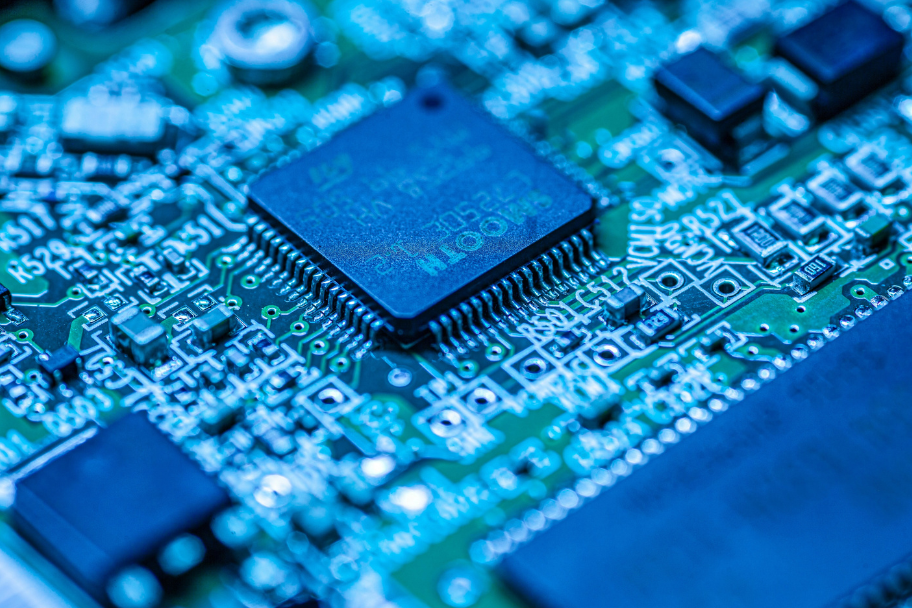
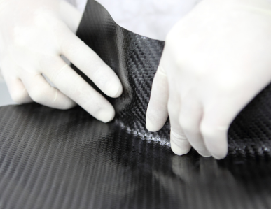
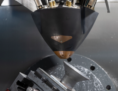
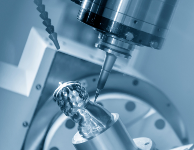
Innovative Communication: Real-time 2D annotation tool now available! ⚡️ Try it now!
Talk to us now
電話アイコン 0120-987-742

Case Studies

Parts Manufacturing for the Electronics and Semiconductor Industry with Taiga | Precision Machining with Quick Turnaround

We provide precision parts for electronics and semiconductor manufacturing with quick lead times. Our high-precision machining technology contributes to miniaturization and enhanced performance.

Prototyping of components for the electronics and semiconductor industries to you

Specializing in the manufacture of components for the electronics and semiconductor industries, our service offers innovative manufacturing solutions to meet the needs of fine and high precision by proposing a variety of processing technologies. We can handle everything from the prototype stage to small lot production, and you can trust our ISO 9001 certified system.

Taiga Application Examples in the Electronics and Semiconductor Industry

  • Electronic circuit boards and cases

    We can manufacture parts that require high precision and precise dimensions.

  • Prototypes and prototypes

    Prototypes and trial products for new products can also be manufactured with short lead times.

  • Cable guides and wiring fixtures

    Flexible shapes can be accommodated for each wiring layout.

Other areas of usefulness include

Nozzles and jigs for semiconductor manufacturing equipment

Insulation materials and spacers

Heat dissipating parts

Key features and benefits of using the Taiga

Suitable for small-lot production

Large-scale production lines are not required. We specialize in flexible small-lot production.

Proposing state-of-the-art technology

3D printing service for multiple materials such as metals, CFRP, and ceramics, enabling precise and complex shapes.

Short delivery time from prototype

We help speed up product development by quickly producing prototypes and trial products.

ISO 9001 certified

In addition to ISO 9001 certification, the product meets manufacturing standards that require high reliability.

No information entry required!

Download >

Click here for registration and questions

Contact >

Examples of technologies utilized in the electronics and semiconductor industries

CFRP加工

CFRP

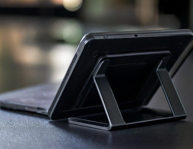
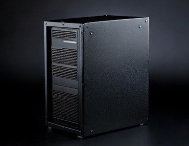
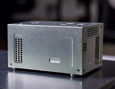
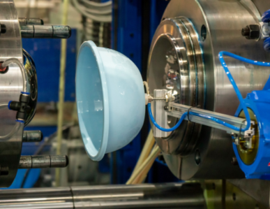
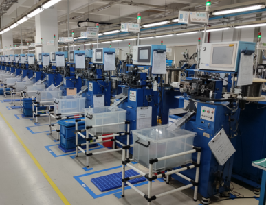
CFRP processing technology is used in electronics and semiconductor manufacturing to achieve lightweight and highly rigid components. For example, CFRP is used in the manufacture of housing parts for precision equipment, arms for transport equipment, frames and stages for mounting equipment, and parts used in static-sensitive environments. CFRP is lighter than metal and has superior vibration damping and dimensional stability, making it ideal for manufacturing electronic devices and semiconductor components that require minute movements and high-speed processing. It also has chemical resistance and non-magnetic properties, making it suitable for use in clean environments.

Learn more about our technology.

金属3Dプリント

Metal 3D Printing

Metal 3D printing is suitable for manufacturing parts with heat-dissipating structures, electromagnetic shield enclosures, and precision fixed parts, enabling the creation of parts that simultaneously satisfy high precision and functionality. Highly thermally efficient products that take advantage of design freedom are ideal for semiconductor devices and electronic equipment, which are becoming smaller and more sophisticated.

Learn more about our technology.

樹脂3Dプリント

Resin 3D Printing

Resin 3D printing is widely used for prototyping electronic device housings, connector covers, and wiring jigs. As components continue to become smaller and more complex, this technology, which combines prototyping speed and flexibility, is making a significant contribution to shortening product development cycles.

Learn more about our technology.

板金加工

Sheet Metal

Sheet metal processing technology is utilized in the manufacture of metal parts that require precision and strength in the manufacture of electronic devices and semiconductors. Typical parts made with sheet metal processing include equipment exterior cases, racks, chassis, cooling fan covers, and power supply unit enclosures. By cutting, bending, and welding metal sheets, such as aluminum and stainless steel, and then fabricating them, parts with high dimensional accuracy can be produced. Designs with heat dissipation and electromagnetic shielding performance can also be accommodated, and anodizing and painting can be applied as exterior finishes.

Learn more about our technology.

切削加工

Machining

Cutting technology is indispensable for manufacturing high-precision and highly reliable components in electronics and semiconductor manufacturing. Typical parts manufactured by cutting include metal spacers for fixing circuit boards, heat sinks for cooling, precision connector parts, mounting plates inside equipment, and frames for optical devices. High-precision machining of aluminum, copper, and resin materials with NC lathes and machining centers enables us to manufacture high-quality electronic devices and semiconductors, even with minute dimensional tolerances. In addition, since stable quality can be ensured even in small lots, it is widely used for everything from prototypes to main products, and is an important processing method that supports the high performance of electronic components.

Learn more about our technology.

射出成形

Injection Molding

Injection molding technology is a processing method used in electronics and semiconductor manufacturing to produce plastic parts with high precision and in large volumes. Specifically, it is employed in the manufacture of connector housings, insulation spacers, cable clamps, enclosure covers, and switch components. By using engineering plastics such as ABS, PC, and PBT, it is also possible to manufacture parts for electronic devices and semiconductor products that require heat resistance, impact resistance, and insulation properties. Integral molding ensures uniform quality even in complex shapes and excellent mass productivity, making it possible to build a highly cost-effective production system for electronic components.

Learn more about our technology.

冷間加工

Cold Forming Process

Cold working is a processing method that plastically deforms materials below their recrystallization temperature, and is widely used in the manufacture of parts for electronic devices and semiconductors. Cold working is a good match for the sports and outdoor industry, where molds, high precision, and high functionality are increasingly being used, and parts must have extremely high precision and quality. Cold working can achieve very high dimensional accuracy and surface finish, which is important in the electronics and semiconductor fields where minute parts and parts with complex shapes are required. Other advantages include suitability for mass production and improved material strength and hardness.

Learn more about our technology.

  • etching process

  • press working

  • wire-cut electric discharge machining

We offer a diverse range of technologies, including

Examples of materials utilized in the electronics and semiconductor industries

  • aluminum alloy

    Aluminum alloys are widely used in components for electronic equipment and semiconductor manufacturing as lightweight materials with excellent heat dissipation and workability. Typical applications include equipment housings, heat sinks, board mounting plates, equipment frames, and structural components for transport units. Due to its high thermal conductivity, aluminum can efficiently diffuse the heat generated by electronic components, leading to stable equipment operation. Another advantage is that it is suitable for a variety of machining processes, including cutting, sheet metal, and surface treatment, and has excellent appearance quality.

  • stainless steel

    Stainless steel is widely used as a material with excellent corrosion resistance, strength, and cleanliness in parts for electronic equipment and semiconductor manufacturing. In particular, it is resistant to rust even in environments where it is exposed to chemicals and moisture, and it is characterized by minimal deformation and corrosion even after long-term use. Major applications include equipment frames, covers, fixtures, and structural components for clean rooms. It is an important material that supports the stability and durability of precision equipment because of its high appearance quality that can be obtained by surface treatment and polishing, as well as its high rigidity and excellent precision retention.

  • engineering plastics

    Engineering plastics such as ABS, PC, and PBT are widely used in electronics and semiconductor manufacturing as materials with excellent insulation, heat resistance, and moldability. The characteristics of major engineering plastics are as follows ABS: With its excellent processability and cost balance, ABS is widely used in the manufacture of housing covers and connector parts. PC (polycarbonate): High impact resistance and transparency, suitable for manufacturing display windows and safety covers. PBT: With excellent heat and chemical resistance, PBT is used in the manufacture of insulating parts around terminals and connectors. These materials can be precision molded and are representative of materials for electronic device components because they can achieve both mass production and reliability.

In addition to this, we can handle all kinds of materials.

Key to success in manufacturing components for the electronics and semiconductor industries

Advanced processing technology

Advanced processing technology is essential for components for electronic devices and semiconductors, which require micron-level precision. For example, in the case of spacers for fixing circuit boards, heat sinks, and connector parts, dimensional errors and shape variations directly affect product performance. Therefore, it is important to ensure high machining accuracy and repeatability using precision machining technologies such as cutting, injection molding, and electrical discharge machining. It is also essential to establish a quality inspection system using 3D measuring machines and image inspection equipment.

Appropriate material selection and insulation/heat dissipation measures

In the manufacture of components for electronic devices and semiconductors, it is extremely important to select the right material for each application and to take measures for insulation and heat dissipation. For example, engineering plastics such as PBT and PC with excellent insulation and heat resistance are suitable for connectors and spacers. On the other hand, aluminum alloys with excellent thermal conductivity should be selected for heat sinks and housings. In some cases, antistatic resins or conductive materials are used to prevent static electricity. Thus, understanding the characteristics of each material and meeting the necessary requirements for heat dissipation, insulation, and chemical resistance will lead to improved product reliability and safety.

Clean manufacturing environment and quality control system

In the manufacture of components for electronic devices and semiconductors, a clean manufacturing environment and a thorough quality control system are essential because microscopic foreign particles and static electricity can cause product defects. First, we work in clean rooms and use dust-proof clothing and air showers to prevent fine particles from getting mixed in with precision parts. In addition, conductive mats and antistatic materials must be used to prevent damage caused by electrostatic discharge. Furthermore, dimensional accuracy and surface conditions must be checked using 3D measuring machines and microscopes during the inspection process to maintain stable quality. These thorough quality control efforts lead to the creation of safe and reliable products.

Flow of using Taiga

1

Sign Up

Contact us to request a registration form, and our team will help you get started.

矢印
2

Upload Your Design

Submit your drawings and project requirements through the platform.

矢印
3

Get Technical Proposals

Receive detailed proposals from multiple companies with advanced technical expertise.

矢印
4

Compare and Collaborate

Use Taiga’s built-in chat and drawing tools to review and discuss proposals with each company.

矢印
5

Place Your Order

Once you’ve chosen the best proposal, place your order directly through Taiga and start production.

No information entry required!

Download >

Click here for registration and questions

Contact >

Frequently Asked Questions

1 Do you support small parts that require high-precision machining? +
Yes, even small parts can be machined with micron-level precision.
2 Can you manufacture using metals with high heat dissipation? +
Yes, we can manufacture components using materials with excellent heat dissipation properties, such as aluminum and copper.
3 Can you custom design a device case? +
Yes, 3D printing technology can be used to manufacture custom cases with a high degree of freedom.
4 How long does it take for delivery? +
Usually within 2 weeks, but depends on the complexity and number of components. Please contact us for details.

Please feel free to contact us for consultation and questions.

No information entry required!

Download >

Click here for registration and questions

Contact >

Latest Blog See All

セラミックの微細加工|メリットや加工方法、業者の選び方を解説
microfabrication 2025.05.01

Microfabrication of ceramics|Explanation of advantages, processing methods, and how to choose a supplier

Ceramics, with their high heat resistance and durability, are materials used in a wide range of fields. In recent years, for the purpose of improving strength and miniaturization, ceramic [...].

3Dプリンティングの後処理方法|失敗しないための注意点を解説
3D printing 2025.05.01

How to Post-Process 3D Printing|Explaining what to do to avoid mistakes

Have you installed a 3D printer but are having trouble getting the desired results? If you are not properly post-processing after modeling [...]...

With technical proposals from professional engineers
New possibilities for prototype development